PCB Development Tutorial
Producing a PCB can leave some people a little unsure of the correct steps, chemicals and equipment required. Here at Modelling Electronics we understand that our customers are hobbyists and for some customers this can be their first time in producing a professional looking PCB. We have put this tutorial together in order to aid your understanding of how to produce a PCB and all the chemicals and equipment required. We have tried to use tools and equipment that that most people will have at home wherever possible so not to increase the cost of what's required.
We understand that some customers may wish to use photo resist coated boards and some may wish to use the standard copper clad boards so we have described both procedures below.
Design your artwork
No matter which procedure you decide is best for you both will require you to design your art work. So people maybe using pre designed artwork which just needs printing. If so you can skip ahead to that step.
When designing your artwork make sure that you are sure the circuit will work, this saves time and money and also remember not to produce track lines that are too thin. These can thin further or fade away during the development and etching stage.
Cutting your copper clad boards
Cutting your boards can be done in various ways. A sharp Stanley knife works by scoring with a ruler where you want to cut the board. This will need to be done a few times until you have cut through or the board is thin enough to snap. Other options are a hack saw.
Copper clad boards designing
If you are producing a simple circuit and you free confident that you can draw this by hand you can use our Plain Copper Clad Boards. To draw your artwork you will need an Etch Resist Marker Pen, make sure your board is cut to size, clean and dry; alcohol cleaning wipes work well to clean any dirt or grease from the boards. On the copper side of the board you can draw your track layout. make sure there are no faint tracks or tracks that are too thin. When you have finished drawing your track all the ink to dry for about 10 minutes. You are now ready to start etching, please skip down to the PCB etching stage of this tutorial.
If you are using our Photo Resist Coated Boards you will need to print your artwork on clear transparent film in order to use your design. We have three types or artwork work film two are for inkjet printers, Jetstar Standard Inkjet Film, Jetstar Premium Inkjet Film and one for laser printers, Laserstar Film. Once you have produced you PCB design and have this printed off, hold it to the light to make sure that it's all printed as your require. If you are happy with how its printed then you are ready to expose your artwork to your board. For this you will need a UV Exposure Unit.
Place your artwork film on the glass surface off your UV Exposure Unit, out of direct light or preferably an dark room with a red light peal the back off your photo resist coated board. Don't exposure your board to light any longer than you have to and get this placed on top of your artwork film with the photo resist side touching your printed design. Close the lid on your exposure unit. Our UV exposure units have a time dial for 6 minutes, this is enough UV exposure time for our boards. Different units may require longer exposure times. Once your UV exposure unit has finished you are now ready to develop your board.
PCB Developing
Once your UV exposure unit has finished leave the lid closed while you prepare the developer solution. We supply a high grade PCB developer Solution that we have found to be the best on the market. Mix your developer solution as per the packet instructions. We have found that this developer works best at room temperature, it slows down the developing time by about 10-15 seconds allowing you that little bit of time to avoid over developing. We supply to sizes of developer trays which can be used for chemical developing and etching, Small PCB Developer Tray and Standard PCB Developer Tray. Once your tack is clear on your board and there is no more Photo resist coating remove your board from the developer solution, use our Plastic Tweezer / Forceps and rinse in cold water immediately. You are now ready for the PCB etching stage.
PCB etching
Photo resist boards only: if you have used photo resist boards you will now need to check your PCB tracks to make sure none of them have faded away. if you find that some tracks have faded or become very thin it's you will need to touch these up with a Etch Resist Marker Pen, first you will need to dry your board with some kitchen towel, once dry touch up and of your PCB tracks and allow the ink to dry for about 10 minutes.
Now that you are ready to etch your board you will need to mix up your PCB etching solution, we don't stock the standard ferric chloride solution we stock a superior safer etching solution, Fine Etch Crystals. Mix the etching crystals according to the packet instructions.
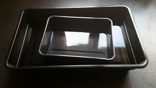
 All etching solution works better when its kept at a temperature of about 45 degrees celsius. Our small developer trays fit nicely on top of a double radiator and this provides a very reliable heat source for the solution. However if it's not cold you don't really want to put the heating on. Another solution is to create bain-marie (Pictured right). This uses both our Small PCB Developer Tray and the Standard PCB Developer Tray, by placing the small developer tray inside the larger tray you can add your etching solution and boards to the small developer tray and filling the larger developer tray with boiling water. this will then heat the etching solution in the smaller developer tray. Etching can take around 40 minutes this way so you may want to change the water in the larger tray a few times. It will seem as nothing is happing for a while then all of a sudden you will start to see white appear around the outside of the board. This is the copper being stripped and leaving the boards plain surface. You will need to agitate the solution from time to time which increases the etching ability. Once etching is completed you will see a white board with just your track layout remaining. Remove the board from the solution, use our Plastic Tweezer / Forceps and rinse in cold water immediately. If you are now ready to clean your board ready for tinning.
There are many chemicals on the market which will remove any leftover photo resist and etch resist maker pen inks but as we have said we are trying to limit the products you need to buy so we have found a cheap solution which most us will have at home. A good nail polish remover which has an acetone content works perfectly. Preferably one used for acrylic nails. Fill one of your small developer tray or a plastic take away tub with a little nail polish remover. Place your board in the solution and with a cotton but give it a quick rub. This only takes seconds and then remove it and rinse in cold water immediately. You are now ready to tin your copper tracks.
Tinning
Tinning is optional but recommended. This puts a tin coating over your copper tracks so that they don't oxidise and bake down over time. We supply a very good tinning solution which is sold in small quantities, Immerse Tin Powder . Mix the immerse tin powder according to the packet instructions. Once your solution is ready pour this into your developer tray and immerse your boards for about 10-15 minutes. ,Use our Plastic Tweezer / Forceps and rinse in cold water immediately. You have now finished with the chemical production side and you can now wash and dry your new printed circuit board. The final step in the PCB production is to apply a green coat to the track side of your board.
PCB Green Coat
Bungard PCB Green Coat is the best product on the market for apply a PCB green coat to the copper track side of your circuit board. It produces a professional, green protective coating for completed PCBs. Subsequent repairs or changes can be simply made through the coating. One of the best product features is that it contains flux and with this added flux it improves solderability. This comes in a small spary can and you simply spray this over your copper track side. Be careful though as you only want a thin coating. Once you have sprayed your boards you need to let them dry. to fully dry and be at its best for soldering you should really leave this for 2-3 days. If you are in a rush you can oven dry but as it's got to be no hotter than 80°C it's not really possible for hobby users as your oven at homes lower temperature is about 110°C. A alternative is to leave it to dry for about an hour and then place this on a warm radiator for 1-2 hours, leave the board to cool and cure for a further 2 hours. Congratulations you are now ready to drill your board and add the components.
If you have any questions about this tutorial please feel free to call us or drop us an email. We are always happy to help and all our staff are trained and do actively produce PCB's.

